- 您现在的位置:买卖IC网 > Sheet目录3882 > PIC16F74T-I/ML (Microchip Technology)IC MCU FLASH 4KX14 A/D 44QFN
2009 Microchip Technology Inc.
DS39682E-page 163
PIC18F45J10 FAMILY
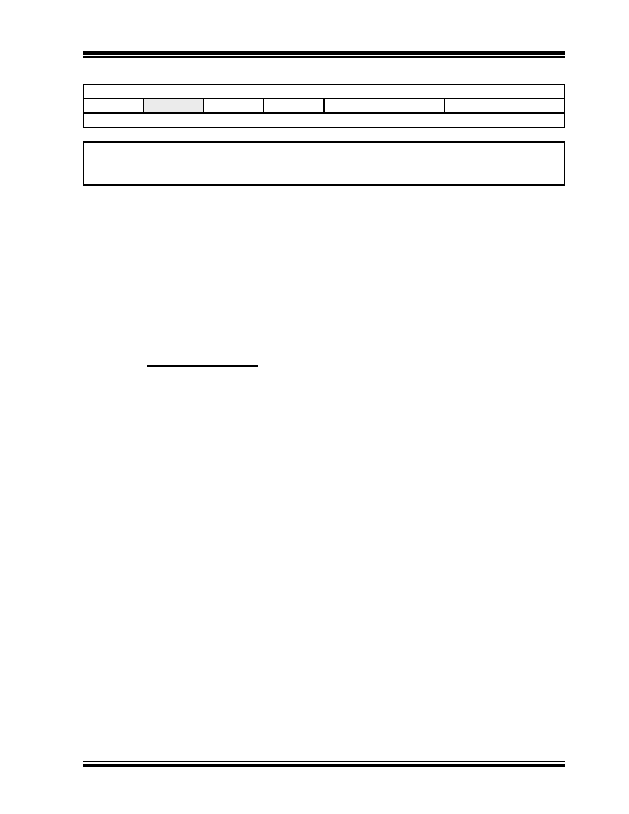
REGISTER 16-6:
SSPxCON2: MSSPx CONTROL REGISTER 2 (I2C SLAVE MODE)
R/W-0
GCEN
ACKSTAT
ADMSK5
ADMSK4
ADMSK3
ADMSK2
ADMSK1
SEN(1)
bit 7
bit 0
Legend:
R = Readable bit
W = Writable bit
U = Unimplemented bit, read as ‘0’
-n = Value at POR
‘1’ = Bit is set
‘0’ = Bit is cleared
x = Bit is unknown
bit 7
GCEN:
General Call Enable bit
1
= Enable interrupt when a general call address (0000h) is received in the SSPxSR
0
= General call address disabled
bit 6
ACKSTAT:
Acknowledge Status bit
Unused in Slave mode.
bit 5-2
ADMSK<5:2>:
Slave Address Mask Select bits
1
= Masking of corresponding bits of SSPxADD enabled
0
= Masking of corresponding bits of SSPxADD disabled
bit 1
ADMSK1:
Slave Address Least Significant bit(s) Mask Select bit
In 7-Bit Addressing mode:
1
= Masking of SSPxADD<1> only enabled
0
= Masking of SSPxADD<1> only disabled
In 10-Bit Addressing mode:
1
= Masking of SSPxADD<1:0> enabled
0
= Masking of SSPxADD<1:0> disabled
bit 0
SEN:
Stretch Enable bit(1)
1
= Clock stretching is enabled for both slave transmit and slave receive (stretch enabled)
0
= Clock stretching is disabled
Note 1:
If the I2C module is active, this bit may not be set (no spooling) and the SSPxBUF may not be written (or
writes to the SSPxBUF are disabled).
发布紧急采购,3分钟左右您将得到回复。
相关PDF资料
PIC16F77T-I/ML
IC MCU FLASH 8KX14 A/D 44QFN
PIC18F24K20-I/SS
IC PIC MCU FLASH 8KX16 28SSOP
PIC16F77-E/ML
IC MCU FLASH 8KX14 A/D 44QFN
PIC16LF74T-I/ML
IC MCU FLASH 4KX14 A/D 44QFN
PIC16F723-I/MV
IC MCU 8BIT 7KB FLASH 28UQFN
PIC18F442T-I/ML
IC MCU FLASH 8KX16 EE A/D 44QFN
PIC18LF2439-I/SP
IC MCU FLASH 6KX16 EE A/D 28DIP
PIC16F687-I/ML
IC PIC MCU FLASH 2KX14 20QFN
相关代理商/技术参数
PIC16F74T-I/PT
功能描述:8位微控制器 -MCU 7KB 192 RAM 33 I/O RoHS:否 制造商:Silicon Labs 核心:8051 处理器系列:C8051F39x 数据总线宽度:8 bit 最大时钟频率:50 MHz 程序存储器大小:16 KB 数据 RAM 大小:1 KB 片上 ADC:Yes 工作电源电压:1.8 V to 3.6 V 工作温度范围:- 40 C to + 105 C 封装 / 箱体:QFN-20 安装风格:SMD/SMT
PIC16F74T-I/PT152
制造商:Microchip Technology Inc 功能描述:
PIC16F74T-I/PTG
功能描述:8位微控制器 -MCU 7KB 192 RAM 33 I/O Lead Free Package RoHS:否 制造商:Silicon Labs 核心:8051 处理器系列:C8051F39x 数据总线宽度:8 bit 最大时钟频率:50 MHz 程序存储器大小:16 KB 数据 RAM 大小:1 KB 片上 ADC:Yes 工作电源电压:1.8 V to 3.6 V 工作温度范围:- 40 C to + 105 C 封装 / 箱体:QFN-20 安装风格:SMD/SMT
PIC16F753-E/ML
制造商:Microchip Technology Inc 功能描述:3.5KB FLASH, 128 RAM, 8MHZ INT. OSC, 9-BIT DAC - Rail/Tube 制造商:Microchip Technology Inc 功能描述:IC PIC MCU 2K FLASH 16QFN 制造商:Microchip Technology Inc 功能描述:8-bit Microcontrollers - MCU 35KB Flsh 128 R 8MHz Int Osc 9-bit DAC
PIC16F753-E/P
制造商:Microchip Technology Inc 功能描述:3.5KB FLASH, 128 RAM, 8MHZ INT. OSC, 9-BIT DAC - Rail/Tube 制造商:Microchip Technology Inc 功能描述:IC PIC MCU 2K FLASH 14PDIP 制造商:Microchip Technology Inc 功能描述:8-bit Microcontrollers - MCU 35KB Flsh 128 R 8MHz Int Osc 9-bit DAC
PIC16F753-E/SL
制造商:Microchip Technology Inc 功能描述:3.5KB FLASH, 128 RAM, 8MHZ INT. OSC, 9-BIT DAC - Rail/Tube 制造商:Microchip Technology Inc 功能描述:IC PIC MCU 2K FLASH 14SOIC 制造商:Microchip Technology Inc 功能描述:8-bit Microcontrollers - MCU 35KB Flsh 128 R 8MHz Int Osc 9-bit DAC
PIC16F753-E/ST
制造商:Microchip Technology Inc 功能描述:3.5KB FLASH, 128 RAM, 8MHZ INT. OSC, 9-BIT DAC - Rail/Tube 制造商:Microchip Technology Inc 功能描述:IC PIC MCU 2K FLASH 14TSSOP 制造商:Microchip Technology Inc 功能描述:8-bit Microcontrollers - MCU 35KB Flsh 128 R 8MHz Int Osc 9-bit DAC
PIC16F753-I/ML
制造商:Microchip Technology Inc 功能描述:3.5KB FLASH, 128 RAM, 8MHZ INT. OSC, 9-BIT DAC - Rail/Tube 制造商:Microchip Technology Inc 功能描述:IC PIC MCU 2K FLASH 16QFN 制造商:Microchip Technology Inc 功能描述:8-bit Microcontrollers - MCU 35KB Flsh 128 R 8MHz Int Osc 9-bit DAC